RF Microwave And Wireless Communication Products
Welcome to our GaAs MMIC package selection guide
if you do not see what you are looking for please send us an email request
RF Microwave And Wireless Communication Products![]()
![]()
Welcome to our GaAs MMIC package selection
guide
if you do not see what you are looking for please send us an email request
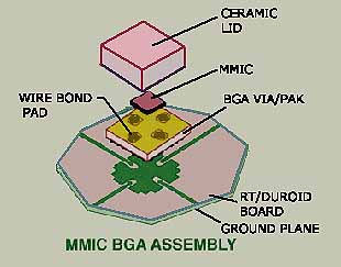
VIA/PAKTM Ball Grid Array (VBGA) Packages for GaAs MMICs From Micro Substrates Corporation and HD Communications MSC's VBGA is an important break through in achieving a true surface-mount packaging solution for high-frequency MMICs. The solution is achieved at an attractive performance/price ratio for the cost-sensitive, commercial wireless market. VBGA packages are manufactured using semiconductor fabrication techniques to achieve the cost advantages of array processing. VIA/PLANE TM, a single layer, ceramic interconnect substrate with tungsten-copper through vias, is the base material for these packages. The balls are brazed to the package using Cu-Ag eutectic alloy. This thin-film, ceramic, surface-mount, VBGA package is developed for applications such as VSAT terminals, point-to-point radio, LMDS, and phased array communication satellites covering a frequency range of DC - 31.5 GHz. A higher frequency VBGA package for 30 - 45 GHz range is currently under development. | |||||||
 |
|||||||
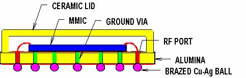
| Completed VBGA Assembly Cross Section | |||||||
The VBGA ceramic substrate is 99.6% alumina, and the high-frequency RF ports are made of specially designed tungsten-copper vias. Additionally, aluminum nitride VBGA ia available for power devices such as power amplifiers. Low-inductance vias, tight impedance control through thin-film process techniques and the elimination of leads ensure high-frequency performance of the package. In addition, ground and DC connections are provided through the tungsten-copper, low-inductance vias, which also ensure good thermal performance. Cu-Ag balls, 0.125mm to 0.25mm high, are the input/output interface to the PC board. Ceramic or plastic lid with epoxy preform can be used for enclosing the MMIC. An outstanding feature of the VBGA is its high degree of flatness to match the IC. This is critical to achieving high assembly yields, especially for flip chips and thin GaAs ICs such as power amplifiers. | |||||||
Comparison of the VBGA with other Microstrip type Packages
Part # 1MSC625B DC-31.5
GHz VBGA Part # 1MSC625B Specifications | ||||||||||||||||||||||||||||||||||||||||
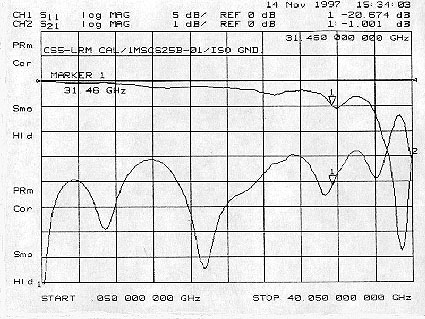
Part # 1MSC625B Performance Chart | ||||||||||||||||||||||||||||||||||||||||
 | ||||||||||||||||||||||||||||||||||||||||
![]()
